(Now a bi-weekly program)
June 4, 2013
Join the "CWTD Yahoo Group" for email discussion in between our bi-weekly sessions.
Analyze This! ... Direct Digital Synthesis with the DDS-60
and
Cool Product of the Month ...SOTAbeams 10m Travel Mast"
Overview
This time we pick up with the popular "Analyze This!" series again with a dissection and analysis of the very popular DDS circuits that serve as local oscillators in many of our homebrew projects these days. While the circuits are relatively small and principles of operation are believed known by most, you might find that some design aspects can surprise you. Whether it is voltage level translation, parasitic oscillations in the post-LPF amplifier, or high current draw and seemingly excessive package temperatures, this episode of CWTD is likely to give you additional considerations when selecting and using a DDS circuit for your next project.
73, George N2APB & Joe N2CX
Podcast -- Listen by clicking the link, or right-click and save to local hard drive for your later listening pleasure.
Sidebar text discussion during the show ...
<20:06:43> "Alan W2AEW": My first time with the DDS-60 (video from a year ago): http://www.youtube.com/watch?v=yxQOSprOo04
<20:13:44> "Clint-ka7oei": There was the DDS in the mid-late 80's by Williams - used 74F283's, IIRC... (It was in QEX, I believe.)
<20:20:47> "Ross vk3ucr": dead mike
<20:28:59> "Ross vk3ucr": Apologies for the audio, refuses to play nice!!
<20:37:53> "George - N2APB": No problem Ross. Still glad you can be with us tonight.
<20:40:22> "Alan W2AEW": The left *half* of the first lobe is called the first Nyquist zone. Ideally, your low pass filter will block the 1st image in the 2nd Nyquist zone
<20:57:05> "Alan W2AEW": ...or, maybe FM the reference input
<21:03:31> "Ken - VA3KMD": The output impedance of the AD8008 is strongly dependent on frequency.
<21:22:32> "Karl W4KRL": Sorry no mic. You said it is important to clear registers at power up. How?
<21:25:24> "George - N2APB": Proper initialization is to first do a clock raise/lower cycle to get the hardware data bits D0, D1 and D2 into the pipeline very first.
<21:25:30> "George - N2APB": Then send 32 zeros followed by 0x01 bit pattern (LSB clocked out first) to set the 6X multiplier.
<21:26:11> "George - N2APB": THEN and only then, you can start programming control words for the frequency desired.
<21:25:43> "Karl W4KRL": Thanks!
<21:26:13> "Howie K3HW": I ordered one Joe - Next shipment of 10 M pole due in at SOTABeams on 6/6/13 - They DO ship to us here in the colonies !!!
<21:26:59> "George - N2APB": The Marx sketch does NOT do this, which is probably the cause for the problems I am having with his sketch.
<21:32:29> "Bob - N2OJJ": I used the 9850 and I think it has a config word setup for 90 degree outputs
<21:34:47> "Ross vk3ucr": The Marx sketch might work ok with the 9850, I understand it uses a different initialization.
<21:36:07> "Armand WA1UQO": As always - Great show tonight! Thanks guys, Be back in two weeks!
Brief History (in relation to ham radio)
N2APB's first experience with a DDS chip ... circa 1995. This was the front panel of a transceiver kit produced by Hands Electronics (in the UK) called the "RMX-10" (??).
Tim Ahrens WB5___ in Texas designed a microcontroller-based front panel containing the AD7008 DDS chip serving as the LO for the radio.
You can see the DDS chip on the backside of the control board as the square 44-pin socketed device just to the left of the white LCD cable ... man, that chip got hot!
Top of the control board
Bottom of the controller board
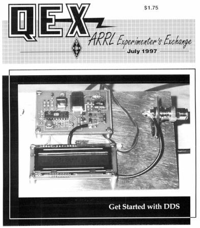
Then the seminal Curtis Pruess WB2V article in QEX for July 1997 introduced many of us to the newer, smaller, faster AD9850 DDS chip,
controlled by the PIC16C54 uC. The article may be downloaded via the links below, and it is a great introduction to one of the very first
mass-constructed DDS chip designs by hams all over the world.
Original DDSVFO Article by Curtis Pruess WB2V, QEX 1997
(Posted with permission from the American Radio Relay League)
JPG & TIF Pages: Page 1 Page 2 Page 3 Page 4 Page 5 Page 6
or Complete article: 8MB PDF file (right-click as safe to your computer)
Later on during 2004-or-so, N2APB and N2CX packaged the AD9850 DDS chip, the necessary LPF and output amplifier
onto a convenient design on a small, pluggable printed circuit board called it the DDS Daughtercard, which was able to
generate good quality sine waves from 1-30 MHz.
Original DDS Daughtercard, aka "DDS-30"
And then we later updated the DDS chip to the faster AD9851 and also went through numerous version the output amplifier (MMIC, discrete transistor,
the LHC-1252, and finally settling on use of the AD8008, a dual op amp with good gain-bandwidth product for stability and low roll-off characteristics to
minimize the effects of sin(x)/x amplitude changes as frequency increases. We dubbed it the "DDS-60" and this has been (and continues to be) available
since then over the years

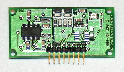
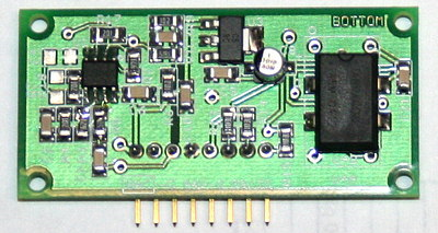
DDS-60 Daughtercard ... (http://midnightdesignsolutions.com/dds60/index.html)
DDS-60 Schematic
Simplicity has been the key to the DDS-60's popularity over the years. Consisting only of the AD9851 DDS chip U2, a clock oscillator module U4,
a low pass filter (LPF) to attenuate sampling artifacts and spurs above the chip's top usable frequency limit (60 MHz), and an RF amplifier that boosts
the DDS's native 250mVpp signal to +/- 4Vpp into a 50-ohm load (40 mW).
The DDS-60 is a self-contained functional module that generates a quality RF signal by using a small pc board containing just the bare DDS essentials – an Analog Devices AD9851 DDS chip, a clock oscillator, a 5th-order elliptic filter and an adjustable-level RF amplifier. Additionally, an onboard 5V regulator is provided so you only need provide a single 12V battery or power supply ranging anywhere from 8-12V DC. The three digital control lines, the power supply, and the output signal are all available on a pin header at the board edge. This 8-position pin header serves to allow the DDS-60 to be plugged into many projects on your bench, regardless of which microcontroller is employed. Just provide a single strip socket (e.g., a 16-pin IC socket split lengthwise) on the project board and plug in the DDS-60. A cable connected to the parallel printer port of your PC can even be used in conjunction with public domain PC software to control the DDS-60. See the Controller section in the full manual for a number of custom solutions illustrating easy control of the DDS-60. Once your controller-of-choice serially loads the control word into the DDS, the raw waveform is generated and presented to an elliptic filter that removes unwanted high-end frequency components, resulting in a signal of sufficient quality to serve as a local oscillator for a transceiver. We regularly see harmonic content down typically more than 40 dB. The signal generated by the DDS is quite small so we use an AD8008 low power amplifier to provide about 18 dB of gain to boost the signal to a maximum of about 4V p-p, which is quite usable for a variety of applications. This amplifier chip offers unconditional stability (k>1) and yields spectrally-clean signals. It is an ideal signal source for making impedance measurements in the Micro908 Antenna Analyst and other demanding applications. A trim pot allows precise manual control of the desired output level. The design accommodates supply voltages ranging from 12V all the way down to 8V, thus conveniently allowing for battery operation. The amplified signal is then available for use as a 50-ohm source input signal. If not used as an input to any other component or module, the output should be terminated with a 50-ohm load for the stated specifications to be realized.
DISSECTING THE DDS-60 CARD
Here we look at each of the four sub-circuits and consider some of the design considerations.
DDS Chip
Discussion points ...
- 5V device
- Built-in 6x clock multiplier
- Reference oscillator U4: max of 180 MHz (x1) or 30 MHz (x6)
- Rset R10 useful pin to control output current to Iout
Low Pass Filter
Discussion points ...
- Zin, Zout = 50 ohms
- Zin || R12 = 24 ohms, balanced by 24-ohm R11 on Ioutb
- Cutoff frequency ~ 70 MHz
Output Amplifier
Discussion points ...
- Capacitively coupled input (C1), output (C7)
- 0.1 uF reactance only acceptable down to ~ 1 MHz, where it gets too large and reduces signal
- Need to raise C1 and C7 to about 10 uF to eliminate signal attenuation below 1 MHz
- Ideally also need to do same for feedback caps C2 and C5 (for gain to be proper)
- 2 stage amplifier for better stability
- R6-R9 divider biases input at 1/2 V+
- AD8008 spec'd at 12V max
- a& b jumper pads originally intended to allow user selection of externally-controlled digipot for gain control, but scheme not good
- R5 establishes Zout ... may want to eliminate (short) this for subsequent stages like a reflectometer.
Power Supply
Discussion points ...
- U3 is a nice 5V, 1A regulator in an SOT223 package
- Caution needed to ensure proper bypassing/filtering on input and output
"I assembled this AMQRP DDS-60 synthesizer kit for a fellow ham. It uses an Analog Devices DDS chip, a reference oscillator, RF output buffer and voltage regulator. I built a quick jig to program the device using the parallel port of an old computer."
"AVR Butterfly DDS-60 by Steve Weber, KD1JV. Constructed by ak2b from QRP radio projects."
Temperature Study
Some builders of the DDS-60 card are surprised at how hot the components operate, particularly the DDS chip (U2) and the 5V voltage regulator device (U3). In quick summary, these components will indeed get pretty warm – in fact too warm to hold your finger on it for more than 5-10seconds – but this is quite normal and here is how we determined that:
DDS-60 card:
Input: 13.4 volts, 128 ma
- Don't forget there's a diode between pwr connector & card, amounting to a 0.2 volt drop.
- This current is for fully operating DDS chip, with PLL turned on effectively creating a 180 MHz ref clock
Regulator:
Input: 13.4 volts
Output: 5 volts, 97 ma
Tj(max) = 150-degC
Theta-JA = 53-degC
AD9851:
Power: 650 mW (worst case from spec sheet, 180 MHz @ 5V)
Tj (max) = 150-degC
Theta-JA = 82-degC
Ambient Temp = 21.1-degC
- - - - - - - - - - -
Theta-JA = Thermal resistance from junction-to-ambient
The all-important equation for Tj (temp of internal semiconductor junction):
Tj = Tambient + (PWR x Theta-JA)
- - - - - - - - - - -
So for the REGULATOR ...Tj = 21.1 + (((13.4 - 5) x .097) x 53) = 64.3-degC
... therefore, compared to Tj(max) of 150, we are well within spec.
And for the AD9851 ...Tj = 21.1 + (.650 x 82) = 74.4-degC
... therefore again, compared to Tj(max) of 150, we are well within spec.
- - - - - - - - - - -
Temperature Measurements ...Tambient = 21.1-degC (70-degF)
Regulator case = 71.1-degC (160-degF)
(Regulator heatsink tab) = 76.6-degC (170-degF)
AD9851 case = 63.9-degC (147-degF)
- - - - - - - - - - -
CONCLUSIONS ...1) The DDS-60 is operating within component thermal and power specifications.
2) The "too hot to touch" cases for the regulator and DDS chips is probably correct. Even my
guitar-calloused fingers cannot be pressed on either of these chips for longer than 10 seconds
without a severe "Ouch!". But this is normal and okay, as long as the ambient temperature stays
below 195-degF (yes, an almost-boiling room temperature will exceed the max Tj of these components!)
The packages are made for this ... our fingers are not.
PS: Voltage, current and temperature measurements made with a Metex ME-11 DVM with a Fluke 80T-150U
temperature probe.
Other DDS Analysis
"Performance of the IQPro DDS VFO and Evaluation of Wideband Opamps", by Gary W. Johnson, WB9JPS
Using the Arduino to Control the DDS-60 Card
Give this one a try yourself! If you've been following along with the Arduino design thread here in CWTD,
this should be a piece o' cake to get working!
http://blog.marxy.org/2008/05/controlling-ad9851-dds-with-arduino.html
(Note: Peter does not have the proper initialization sequence for the AD9851 in his sketch at this page and the code does not often work.
We added the initialization code and things work well now ... see the modified Arduino sketch. )
Sketch ... Sweeps DDS frequency from 10.000 MHz to 10.001 MHz (1 kHz). Easily hear in receiver tuned to 10 MHz


